Apr 15, 2026
- Products & Solutions
- Press Releases
- Media & Entertainment
Mar 12, 2018
Products & Solutions / Press Releases
- A presentation panel to be exhibited at SEMICON China 2018 scheduled to start in Shanghai from March 14 -
Tokyo, Japan - Panasonic Corporation, and Tokyo Seimitsu Co., Ltd. (hereinafter Tokyo Seimitsu) today announced that Tokyo Seimitsu and Panasonic's subsidiary's company, Panasonic Smart Factory Solutions Co., Ltd. (hereinafter PSFS) have started taking orders for the AL300P, Laser patterning machine for Plasma dicing process jointly developed by the two companies. The AL300P is a new product designed for the Plasma dicing process that achieves chips to be diced from a silicon wafer without damage.
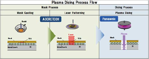
This is a Laser patterning machine developed exclusively for PSFS's Plasma dicing machine (APX300). The AL300P enables a silicon wafer, to which a resist or other mask layer is attached in the pre-processing stage of Plasma dicing, to be patterned at the dicing position with the specified width and high precision through UV Laser processing.
PSFS has equipped the AL300P Laser patterning machine to its Plasma dicing demonstration center in Kadoma City, Osaka, establishing a framework whereby the AL300P can be tested together with PSFS's Plasma dicer APX300 (DM option).
Tokyo Seimitsu plans to exhibit a presentation panel on the AL300P Laser patterning machine at SEMICON China 2018 scheduled to be held in Shanghai, China, from March 14 (Wednesday) through 16 (Friday), 2018.

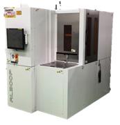
Tokyo Seimitsu's Laser patterning machine AL300P

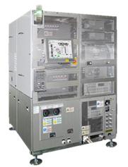
Panasonic Smart Factory Solutions'
Plasma dicer APX300 (DM Option)

The content in this website is accurate at the time of publication but may be subject to change without notice.
Please note therefore that these documents may not always contain the most up-to-date information.
Please note that German, Spanish and Chinese versions are machine translations, so the quality and accuracy may vary.