
FUJIFILM Corporation (President: Shigehiro Nakajima) and Panasonic Corporation (President: Kazuhiro Tsuga) have developed organic CMOS image sensor technology that uses an organic photoelectric conversion layer with a photoelectric conversion property at the light receiving section of an image sensor to achieve performance beyond that of conventional image sensors(*2). Applying this technology to the image sensors of digital cameras and other imaging devices expands its dynamic range(*3) and enhances sensitivity (*4) further to prevent highlight clipping in bright scenes and capture a dark subject with vivid colors and rich textures.
The industry has put into continuous efforts to explore image sensor technologies for increasing their number of pixels. This has dramatically improved sensor resolutions, but, in order to further boost image quality, it is necessary to expand the dynamic range, enhance sensitivity and prevent cross-talk or color mixing between pixels. Panasonic took advantage of its semiconductor device technology to boost image quality for its high-performance image sensors. Fujifilm, on the other hand, has developed highly-reliable organic photoelectric conversion layer with high absorption coefficient to be used on a sensor's light receiving section instead of silicon photodiode(*5) in its effort to build a new image sensor technology.
In the latest collaboration, Fujifilm and Panasonic have combined Fujifilm's organic photoelectric conversion layer technology with Panasonic's semiconductor device technology to jointly develop an organic CMOS image sensor that outperforms conventional image sensors. The new organic CMOS image sensor offers the industry's highest dynamic range of 88dB, advanced sensitivity 1.2 times more sensitive than conventional sensors(*2) and broader range of incident angle(*6) to enable the production of more sensitive and compact cameras with better image quality.
The two companies will promote the application of this organic CMOS image sensor technology to a wide range of products including security cameras, in-vehicle cameras, mobile device and digital cameras.
Fujifilm and Panasonic will present the research results at the 2013 Symposium on VLSI Technology (VLSI2013) to be held in Kyoto on June 11, and the 2013 International Image Sensor Workshop to be held in Utah, U.S.A. on June 15.
(*1) Performance of the light receiving section of image sensors, as of June 11, 2013 according to Panasonic data.
(*2) Estimation from Panasonic image sensors
(*3) Range of light that can be recorded (ratio between the brightest and darkest areas recorded)
(*4) The sensitivity of image sensors refers to the conversion ratio of light into electric signals. The greater the sensitivity is, the clearer you can capture low-light scenes.
(*5) A type of photo detector that senses incident light, installed for each image sensor pixel to convert light into electric signals
(*6) Range of incident light angles for efficient conversion into electric signals
<Overview of the newly-developed organic CMOS image sensor technology>
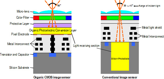
A conventional image sensor consists of a silicon photodiode for capturing light, metal interconnect, color filter and on-chip micro-lens. The newly-developed organic CMOS image sensor technology uses organic photoelectric conversion layer with high absorption coefficient instead of the silicon photodiode, reducing the thickness of the light receiving section down to 0.5 microns, i.e. one severalth of the thickness of a silicon photodiode. This structure provides the following benefits:
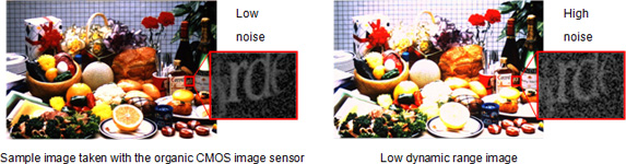
(1) Industry's highest dynamic range of 88dB to prevent highlight clipping and produce a vivid and texture-rich image even in low light
- Panasonic's semiconductor device technology has improved the signal saturation value(*7) by four folds compared to that of conventional image sensors. Coupled with the newly-developed noise-cancelling circuit, the sensor technology provides the industry's highest dynamic range of 88dB, preventing highlight clipping in bright scenes and capturing a vivid and texture-rich image in low light.
(*7) The maximum amount of electric signals that can be handled. Receiving a signal greater than this value leads to highlight clipping.
(2) 1.2 times higher sensitivity than conventional sensors to capture clear images even in low light
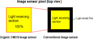
- The transistors and metal interconnects in each pixel, fabricated using Panasonic's semiconductor device technology, are coated with photoelectric conversion layer, developed using Fujifilm's organic material technology. The area of the light receiving section becomes limited in conventional image sensors because of the existence of metal interconnects and the need to form light shield film to prevent light incidence into areas other than the photodiode in each pixel. However, the organic CMOS image sensor technology coats the sensor with organic film, which can harvest all the light received on the sensor. This boosts sensor sensitivity by 1.2 times compared to conventional sensors to deliver clear images even in low light.
(3) Range of incident angle expanded to 60 degrees for faithful color reproduction (*See the image sensor illustrations on the previous page)
- The thickness of the organic film with high absorption coefficient, developed by Fujifilm, has been reduced to just 0.5 microns, or one severalth of the thickness of silicon photodiode in the light receiving section. Since the conventional silicon photodiode measures at least 3 microns in depth, the range of incident angles was limited to around 30 - 40 degrees. The thin film, achieved with the organic CMOS image sensor technology, has enabled the expansion of this range to 60 degrees, efficiently utilizing light entering at an angle for faithful color reproduction with no color mixing. It also gives greater flexibility in lens designs, facilitating the reduction of overall camera size.
(4) Offering high reliability for broader applications
- Fujifilm has developed a process technology to produce inorganic films for protecting the organic film. It prevents the entry of moisture and oxygen into the organic film to safeguard it against performance degradation. The sensor technology has cleared reliability tests involving the application of stress such as temperature, humidity, electrical voltage and light, paving the way for the use of the organic CMOS image sensor in a wide range of applications.
About FUJIFILM Corporation
FUJIFILM Corporation is one of the major operating companies of FUJIFILM Holdings. Since its founding in 1934, the company has built up a wealth of advanced technologies in the field of photo imaging, and Fujifilm is now applying these technologies to other new business fields. Fujifilm brings continuous innovation and leading-edge products to a broad spectrum of industries including medical systems / life sciences, graphic arts, document solutions, highly functional materials, optical devices and digital imaging. Fujifilm aims to help enhance the quality of life of people worldwide by providing top-quality products and services with its leading-edge, proprietary technologies. Through its corporate philosophy, Fujifilm demonstrates its commitment to making a significant contribution to society. For more information, please visit http://www.fujifilm.com.
About Panasonic
Panasonic Corporation is a worldwide leader in the development and engineering of electronic technologies and solutions for customers in residential, non-residential, mobility and personal applications. Since its founding in 1918, the company has expanded globally and now operates over 500 consolidated companies worldwide, recording consolidated net sales of 7.30 trillion yen for the year ended March 31, 2013. Committed to pursuing new value through innovation across divisional lines, the company strives to create a better life and a better world for its customers. For more information about Panasonic, please visit the company's website at http://panasonic.net/.
Media Contacts:
- Tokyo Public Relations Office
- Panasonic Corporation
- Tel: +81-3-3574-5664 Fax: +81-3-3574-5699
- Panasonic News Bureau
- Tel: +81-3-3542-6205 Fax: +81-3-3542-9018


![[Video] TOYOTA ARENA TOKYO is born! Where next-gen sports experiences happen](http://news.panasonic.com/uploads/tmg_block_page/cover_image/18092/tat-main.jpg)
