![[Video] Panasonic Stories in 60 Sec: The Process of Creating the Future](http://news.panasonic.com/uploads/tmg_block_page/cover_image/18585/60sec-the-process-of-creating-the-future-en.jpg)


Feb 24, 2026
- Products & Solutions
- Press Releases
Apr 16, 2021
Products & Solutions / Press Releases
Osaka, Japan - Panasonic Corporation has developed a manufacturable technology to drastically improve the device performance fabricated on silicon (Si) wafers by leveraging the unique feature of a phononic crystal structure*2, which can break the classical limitation of heat insulation property of solids*3. By introducing this technology to a thermal-type far infrared sensor, heat loss from the infrared-receiving section was reduced approximately to 1/10 of the initial sensor without the phononic crystal structure. As a result, infrared detection sensitivity was improved nearly by a factor of 10 in the sensors with phononic crystals. Panasonic presented this world's first research result on phononic far infrared sensors as an invited talk at SPIE Defense + Commercial Sensing 2021, which is one of the five major conferences of the SPIE (the international society for optics and photonics) in the fields of optics, photonics, and image engineering.
In the AI and IoT era, electronic devices tend to be packaged smaller and in higher density than ever. Increase in hot spots and unexpected heat flow in these devices have been a major concern as they can easily disturb the device performances. Therefore, development of an innovative thermal management technology is highly demanded for next generation microelectronic devices.
Recent studies have revealed that the classical limitation of thermal insulation performance of solids can be broken in an artificial structure with nanometer-scale periodic elastic continuum. Such artificial periodic structures are called phononic crystals, which allow for manipulating the propagation of phonons that dominate the thermal properties of semiconductors. However, extremely fine nanostructure patterns in the order of sub-50 nm are necessary to maximize the thermal insulation performance of phononic crystals. This feature made it difficult to employ the standard microfabrication tools used in conventional semiconductor foundries, which had hindered the practical leveraging of the unique feature of phononic crystals to electronic devices.
Panasonic developed a technology to fabricate phononic crystal structures in which the diameter and the period of pores are precisely controlled in the order of several tens of nanometers. The technology developed here is applicable to mass production on Si wafers. This newly developed technology enables the company to enhance the thermal insulation perfomance of Si thin films by a factor of ten. Panasonic has adopted this technology to Si supporting legs of infrared sensors (Fig. 1) to significantly improve the thermal insulation performance and to incerase the temperature rise of the infrared-receiving section upon infrared absorption (Fig. 2). This eventually led to improvement of the infrared detection sensitivity by a factor of ten (Fig. 3).
Utilizing this technology, Panasonic will provide new thermography solutions with higher temperature resolutions and innovative thermal management solutions in microelectronic devices through exploring the possibilities of collaboration with partners.
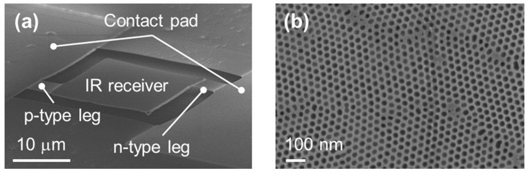 Figure 1: SEM*4 images of the phononic far infrared sensor. (a) Bird-eye view of the phononic infrared sensor. (b) Magnified view of the phononic crystal structure on the supporting leg.
Phononic crystal structures with sub-100 nm periodicity are usually fabricated by an electron beam lithography*5 nanopatterning process. However, in electron beam lithography, the patterns are fabricated by scanning the focused electron beam in two-dimensions. The scanning process in electron beam lithography restricts the throughput for mass production. Panasonic has adopted a block copolymer*6 self-assembly process*7 for phononic crystal fabrication, which is highly applicable to mass production. In a collaborative research with the University of Chicago, Panasonic has succeeded in reducing the cylinder structure of phononic crystals with a diameter of 26 nm and a periodicity of 38 nm, thereby breaking the classical limitation of the thermal insulation performance of bulk Si.
Panasonic has successfully transferred the self-assembly pattern of block copolymers on the supporting legs of far infrared sensors fabricated on Si (100 nm) / SiO2 (2000 nm) / Si wafers. The thermal conductivity of Si thin films was reduced from 31.2 W/mK to 3.6 W/mK by the introduction of the phononic crystal structure. The thermal insulation performance achieved in the company’s phononic crystal is much greater than that achieved in classical porous Si. Figure 2 shows the simulated temperature distribution of the infrared sensor with and without phononic crystals upon absorption of infrared radiation. Panasonic sees a huge increase in temperature rise of the infrared receiving section of the phononic infrared sensor due to enhancement in its thermal insulation performance. The company demonstrates that its phononic far infrared sensor can be much sensitive in infrared detection than in the standard infrared sensors.
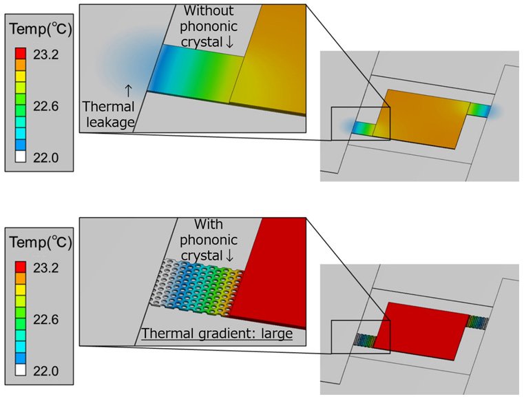 Figure 2: Comparison of temperature distribution of infrared sensor with and without a phononic crystal structure upon absorption of infrared absorption.
Note: Phononic crystal structure effectively hinders the propagation of phonons in a completely new fashion breaking the classical limitation of thermal insulation performance in porous media.
Thermoelectric voltage of infrared sensors with and without phononic crystals were measurement upon heating the infrared receiver by an infrared laser (Fig. 3). Panasonic found that the thermoelectric voltage of phononic far infrared sensors was approximately ten times higher than that of the nonporous sensor without a phononic crystal structure. This result demonstrates the potential of phononic crystals to enhance the infrared detection sensitivity.
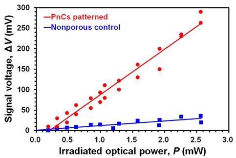 Figure 3: Thermoelectric voltage generated in infrared sensors with and without phononic crystals measured as a function of incident laser power.
Note: The infrared-receiving section shown in Fig. 1 is heated by an infrared laser, and the thermoelectric voltage generated between the two electrodes is measured.
Panasonic Corporation Brand Strategy Division Corporate PR Department
https://news.panasonic.com/global/contacts/
Panasonic Corporation is a worldwide leader in the development of diverse electronics technologies and solutions for customers in the consumer electronics, housing, automotive, and B2B businesses. The company, which celebrated its 100th anniversary in 2018, has expanded globally and now operates 528 subsidiaries and 72 associated companies worldwide, recording consolidated net sales of 7.49 trillion yen for the year ended March 31, 2020. Committed to pursuing new value through innovation across divisional lines, the company uses its technologies to create a better life and a better world for its customers. To learn more about Panasonic: https://www.panasonic.com/global.
The content in this website is accurate at the time of publication but may be subject to change without notice.
Please note therefore that these documents may not always contain the most up-to-date information.
Please note that German, Spanish and Chinese versions are machine translations, so the quality and accuracy may vary.