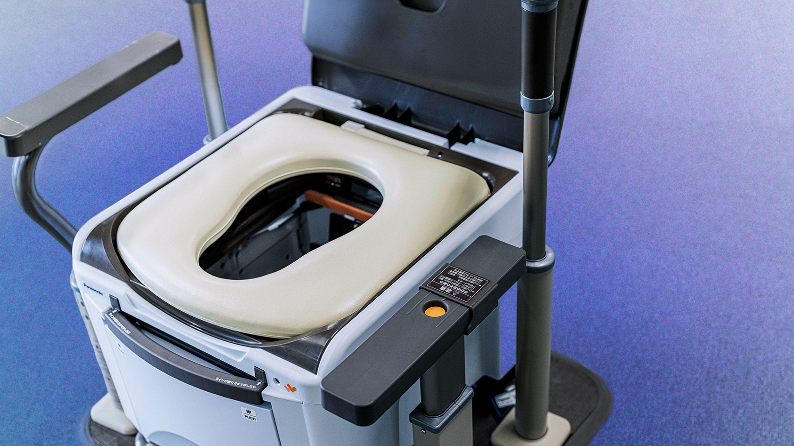
![[Video] Panasonic HX in Action: Demonstrating Hydrogen Solutions in Europe](http://news.panasonic.com/uploads/tmg_block_page/cover_image/18213/hx-video-main.jpg)

Dec 25, 2025
- Products & Solutions
- Stories
- Technology
- AI & Robotics
- R&D
- Business Solutions
May 30, 2016
Products & Solutions / Press Releases
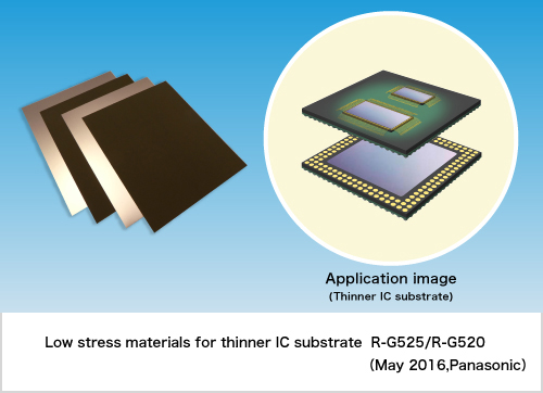
Panasonic's new substrate material is suited to a wide variety of semiconductor packages, leading to faster material selection and greater design freedom.
Osaka, Japan - Panasonic Corporation announced today that it has developed the MEGTRON GX series (product No. R-G525/R-G520), a substrate material that allows thinner and less expensive semiconductor packages for application to a wide range of semiconductor packages (PoP [1], MCP [2], etc.). Panasonic will start mass-producing the new material in June 2016. This substrate material, the embodiment of a completely new idea, shows reduced internal stress [3] that risks causing warpage, and is applicable to a wide variety of semiconductor packages, allowing faster material selection and improved design freedom. The new product also provides highly reliable connections between IC chips and package substrates.
With mobile equipment becoming ever thinner and more sophisticated, urgent studies are ongoing to develop new types of semiconductor packages. Today, substrate materials with different coefficients of thermal expansion (CTE) [4] are needed for different types of semiconductor packages, making material selection and matching very time-consuming. By utilizing a resin technology designed to minimize internal stress, Panasonic has commercialized a new substrate material that is applicable to a wide range of semiconductor packages.
The substrate material is for use in thin semiconductor packages incorporated in mobile equipment such as smartphones and tablets.
The product will be exhibited at ECTC 2016, held at the Cosmopolitan of Las Vegas in the US from May 31 to June 3, 2016, and at the JPCA Show 2016, held at Tokyo Big Sight, from June 1 to June 3.
The continuing trend of manufacturing thinner semiconductor packages has led to a demand for minimal warpage of package substrate material. Having devised the resin design technology to eliminate internal stress, Panasonic has succeeded in reducing the variation in warpage of the substrate material to 110 μm (for a 160 μm-thick substrate and a 100 μm-thick chip) when the material's temperature is increased from 25℃ (room temperature) to 260℃. This substrate material, due to its smaller warpage, assists the manufacture of thinner semiconductor packages.
Currently, different types of semiconductor packages (PoP, MCP, etc.) require substrate materials with different CTEs, which take longer to identify and select. The newly developed low-stress substrate material reduces the warpage of IC chips and package substrates, regardless of their thickness or chip sizes, allowing it to be applied to a wide range of semiconductor packages. This speeds up the selection of package substrate material and gives greater design of freedom.
Conventional substrate material includes an insulating layer composed of resin and glass cloth. Low CTE glass cloth, special one is an expensive material that is used to reduce the CTE, but it is the commonest method adopted to suppress warping of the substrate material. The developed substrate material minimizes warpage with the standard glass cloth, not special one due to its newly-adopted resin design technology, thus cutting the cost of the semiconductor package. The new substrate material is applicable to a wide range of semiconductor packages, opening the way to far simpler management of substrate materials inventory with different coefficients of thermal expansion (CTE) for different semiconductor packages.

Panasonic Corporation is a worldwide leader in the development of diverse electronics technologies and solutions for customers in the consumer electronics, housing, automotive, enterprise solutions and device industries. Since its founding in 1918, the company has expanded globally and now operates 474 subsidiaries and 94 associated companies worldwide, recording consolidated net sales of 7.553 trillion yen for the year ended March 31, 2016. Committed to pursuing new value through innovation across divisional lines, the company uses its technologies to create a better life and a better world for its customers. To learn more about Panasonic: http://www.panasonic.com/global.
Panasonic Corporation
Tel: +81-(0)3-3574-5664 Fax: +81-(0)3-3574-5699
The content in this website is accurate at the time of publication but may be subject to change without notice.
Please note therefore that these documents may not always contain the most up-to-date information.
Please note that German, Spanish and Chinese versions are machine translations, so the quality and accuracy may vary.