![[Video] Panasonic HX in Action: Demonstrating Hydrogen Solutions in Europe](http://news.panasonic.com/uploads/tmg_block_page/cover_image/18213/hx-video-main.jpg)

Dec 25, 2025
- Products & Solutions
- Stories
- Technology
- AI & Robotics
- R&D
- Business Solutions
May 26, 2016
Products & Solutions / Press Releases
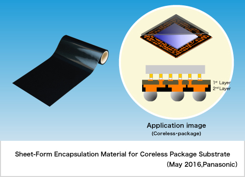
Panasonic's new material for coreless package substrates is suited for the insulation layer of semiconductor package substrates.
Osaka, Japan - Panasonic Corporation announced today that it has developed a sheet-form encapsulation material (CV2008 series) for coreless package substrates [1] that enables thinner-profile and lower-cost semiconductor packages. The sheet-form encapsulation material, scheduled for mass production from June 2016, is optimized for the insulation layers of coreless package substrates. Its suitability for large-area encapsulation allows thinner packages to be manufactured at lower cost.
With the increasing compact-sizing and ever-higher functionality of mobile terminals such as smartphones, the packages used in these products need to have thinner profiles and lower cost. One noticeable response to this demand has been to develop a new coreless process that differs from the current mainstream buildup process using thin core materials[2]. The market requires an insulation material for coreless processes that shows good productivity and eliminates the need for thin core materials as well as laser drilling processing. Panasonic has responded by using its resin design technology to develop a sheet-form encapsulation material for coreless package substrates.
Copper pillar resin encapsulation type coreless package substrates, etc.
This product will be exhibited at ECTC 2016, to be held at The Cosmopolitan of Las Vegas, Nevada, USA, from May 31 to June 3, 2016.
Conventional package substrates are produced from thin core material including glass cloth, and via [3] forming requires laser drilling processing and through-hole copper plating for connection between both surfaces, resulting in a high-cost process. In contrast, a coreless package substrate using the new copper pillar resin encapsulation process [4] can produce copper pillars by copper plating employing an additive process that eliminates the need for laser drilling processing, leading to a thinner package profile and lower cost. To enable the mass production of package substrates, an easily-managed material is needed that allows the press-forming of a uniform insulation layer over a large area. Panasonic has commercialized a product featuring sheet-formed encapsulation material of uniform thickness that is optimized for coreless processes by applying a unique filler design and proprietary resin design technology. Adoption of this material for the insulation layer enables press forming over a large area, contributing to the mass production of packages at lower cost. Sheet thicknesses from 20 µm to 200 µm can be produced for the wide variety of package types required by customers.
A coreless package substrate carries the risk of increased warpage if its insulation layer is very thin, risking handling problems during the assembly process. To secure reliability in the assembly process, minimal warpage is required, especially for a thin material. The company's unique filler design and resin design technology have achieved high rigidity and strength even with extremely thin sheets, reducing package warpage while maintaining a thin profile.
Since the package assembly process may undergo multiple high temperature reflow processes, a smaller thermal shrinkage rate is required for package substrate materials to prevent bonding defects between the conductor on the substrate and the IC chip. This material has achieved a low shrinkage rate by developing a unique filler design technology that will achieve improved production yield in the assembly process.

Panasonic Corporation is a worldwide leader in the development of diverse electronics technologies and solutions for customers in the consumer electronics, housing, automotive, enterprise solutions and device industries. Since its founding in 1918, the company has expanded globally and now operates 474 subsidiaries and 94 associated companies worldwide, recording consolidated net sales of 7.553 trillion yen for the year ended March 31, 2016. Committed to pursuing new value through innovation across divisional lines, the company uses its technologies to create a better life and a better world for its customers. To learn more about Panasonic: http://www.panasonic.com/global.
Panasonic Corporation
Tel: +81-(0)3-3574-5664 Fax: +81-(0)3-3574-5699
The content in this website is accurate at the time of publication but may be subject to change without notice.
Please note therefore that these documents may not always contain the most up-to-date information.
Please note that German, Spanish and Chinese versions are machine translations, so the quality and accuracy may vary.