![[Video] Panasonic Stories in 60 Sec: The Process of Creating the Future](http://news.panasonic.com/uploads/tmg_block_page/cover_image/18585/60sec-the-process-of-creating-the-future-en.jpg)

Apr 15, 2026
- Products & Solutions
- Press Releases
- Media & Entertainment
Oct 12, 2016
Products & Solutions / Topics
Panasonic Factory Solutions Co., Ltd.
One-stop Process Evaluation
Available October 12, 2016
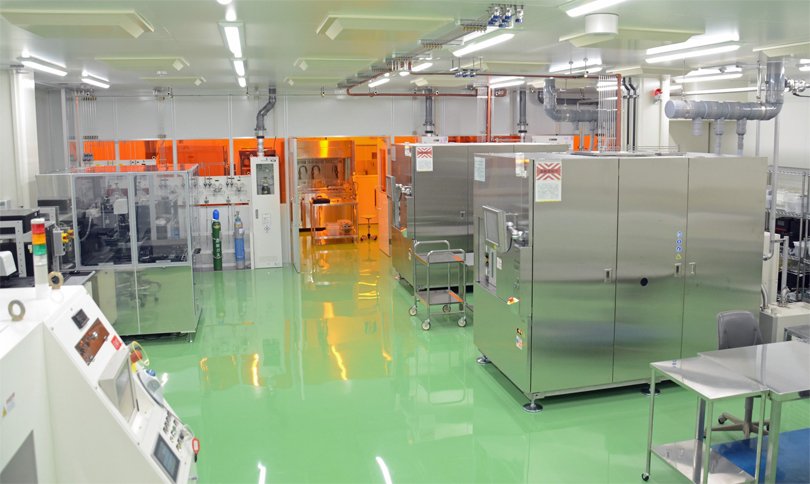
Panasonic Factory Solutions Co., Ltd., a business unit of Panasonic Corporation, announces today the opening of their "Plasma Dicing Demonstration Center" in Osaka, Japan. The center is established to promote a new plasma dicing process to dice silicon wafers thinned to 25μm, which is half the thickness of current memory products.
The center's clean room is showcasing a vertically integrated processing and inspection equipment dedicated for supporting the plasma dicing process. The one-stop process center eliminates the need for the customer to conduct wafer sample preparation at multiple sites and ensuring protection of their highly confidential information.
The center provides the capability to develop processes for new wafer structures and materials. Panasonic will utilize this center as a development site for plasma dicing technology.
Core equipment in plasma dicing process
High speed, non-contact, damage free and enabling narrow dicing street width of 20μm (aspect ratio 5:1) for 100μm thinned silicon wafers and challenging 25μm thinned wafers.
Back grinder:Process to make wafers thinner to a specified value
Lithography:Form protective layer from plasma exposure
Laser patterning:Creating lines for plasma dicing
Measurement of the difference in level and thickness, Electron microscope
Outline of Plasma dicing demonstration center
|
Opening period |
October 12, 2016 |
|---|---|
|
Address |
2-7 Matsuba-cho, Kadoma City, Osaka 571-8502, Japan |
|
Square footage |
Approximately 220 square meter, class 1000 clean room and process preparation room |
Kato / Chanomae
Business Innovation Center, Smart Factory Solutions Business Division,
Panasonic Corporation
TEL : 050-3487-5862 / 050-3688-0603
Akio Kaneko
Corporate Planning Group
Panasonic Factory Solutions Co., Ltd.
TEL : 050-3487-3587
To facilitate the IoT, thinner and smaller semiconductor chips are required which bring major impact to conventional manufacturing. Especially in the blade dicing methods, there are mechanical damage challenges such as edge chipping and side wall damage during mechanical dicing. As chip size decrease, blade width have a greater impact on chip yield per wafer. In addition, the mechanical dicing method leaves mechanical residue and requiring water cleaning steps; a detriment to image sensors. There are well-known challenges and principle limitations on blade dicing methods. For those reasons, there is a growing expectation to refine the plasma dicing process.
Plasma dicing technology is non contact process via plasma reaction to dice chips without damage. It enables narrow-width processing which increases yield of harvested chips from a wafer. Furthermore, plasma dicing does not leave mechanical residue on wafers. It is a method solving dicing challenges for the future.
Blade dicing
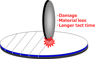
Mechanical contact processing
Plasma dicing
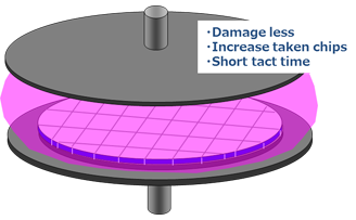
Non contact processing by chemical reaction
Plasma dicing features:
(1)Damage free
Plasma dicing is a noncontact process by chemical reaction so it will not cause mechanical damage to the wafer.
[Examples of application area] Memory, Image sensor
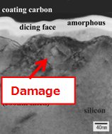
Blade Process
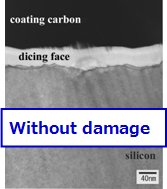
Plasma Process
Magnified photograph of silicon chip sidewall after dicing
(Observed by Transmission electron microscope)
(2)Reduces material loss, increases chip yield
Plasma dicing enables under 20μm dicing width whereby increasing the usable wafer area and increasing the chip yield per wafer. Plasma dicing is a parallel batch process with shorter cycle time compared to the traditional blade method which is a series of vertically and horizontally mechanical motions.
[Examples of application area] Chip component, RF-ID tag
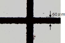
Blade Process
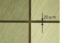
Plasma Process
Magnified photograph of silicon chip surface after dicing
(Observed by optical microscope)
(3)Plasma dicing do not leave mechanical residue on wafer
Mechanical residue after mechanical dicing is the major contributor for image sensor failure and other MEMS devices. Plasma dicing method is clean and do not require post water cleaning steps.
[Examples of application area] Image sensor
Plasma Dicing Demonstration Center
The content in this website is accurate at the time of publication but may be subject to change without notice.
Please note therefore that these documents may not always contain the most up-to-date information.
Please note that German, Spanish and Chinese versions are machine translations, so the quality and accuracy may vary.