Jun 02, 2026
- Products & Solutions
- Press Releases
- Business Solutions
Feb 08, 2018
Products & Solutions / Press Releases
Panasonic will launch the mass production of molded underfill semiconductor encapsulation materials in Shanghai, China in response to the increased production of leading-edge semiconductor packages in the region. This added capacity will enable Panasonic to provide faster and more efficient service to customers in China.
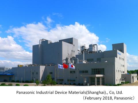
Osaka, Japan - Panasonic Corporation announced today that Panasonic Industrial Devices Materials (Shanghai) Co., Ltd. (PIDMSH) will start high-volume manufacturing of molded underfill (MUF)[1] materials for advanced semiconductor packages in March 2018 in response to the increasing demand for these products in China.
Along with the increasing domestic demand and growing exports, Chinese electronics manufacturers are increasing production of smartphones and other portable electronic devices. As a result, outsourced semiconductor assembly, test contractors(OSATs) and other semiconductor manufacturers are boosting their production volumes. The higher performance and increased functionality of new smartphones is driving high-density semiconductor packaging technology development. As a result,, demand for MUF materials is growing. To provide faster and more efficient service for semiconductor packaging customers in China, Panasonic will launch the production of MUF materials at PIDMSH in March 2018.
MUF materials are designed to encapsulate and protect the Flip chip semiconductor die and the electrical connections between the die[2] and the semiconductor package circuit board. MUF materials encapsulate the entire semiconductor package without the need for a subsequent underfilling process.
In addition to the production site in China, Panasonic produces MUF materials in Yokkaichi-city, Mie Prefecture in Japan.
| Company name | Panasonic Industrial Devices Materials (Shanghai) Co., Ltd. |
|---|---|
| Location | 148, Huancheng North St., Comprehensive Industrial Development Zone, Shanghai, China |
| Founded | October 2001 |
| Representative | Takashi Sakamoto (General Manager) |
| Main production items | Thermosetting resin molding compounds (heat-resistant phenolic resin molding compounds for automotive electric system parts, etc.), engineering plastics, and semiconductor encapsulation materials (* MUF materials production will start in March 2018) |
Panasonic's MUF materials will be exhibited at SEMICON China 2018 from March 14 to 16, 2018 at the Shanghai New International Expo Center.
Panasonic Corporation is a worldwide leader in the development of diverse electronics technologies and solutions for customers in the consumer electronics, housing, automotive, and B2B businesses. Celebrating its 100th anniversary in 2018, the company has expanded globally and now operates 495 subsidiaries and 91 associated companies worldwide, recording consolidated net sales of 7.343 trillion yen for the year ended March 31, 2017. Committed to pursuing new value through innovation across divisional lines, the company uses its technologies to create a better life and a better world for its customers. To learn more about Panasonic:
http://www.panasonic.com/global
Panasonic Corporation
Tel: +81-(0)3-3574-5664
The content in this website is accurate at the time of publication but may be subject to change without notice.
Please note therefore that these documents may not always contain the most up-to-date information.
Please note that German, Spanish and Chinese versions are machine translations, so the quality and accuracy may vary.