Nov 18, 2025
- Products & Solutions
- Stories
- Operating Company
Feb 03, 2016
Products & Solutions / Press Releases
Osaka, Japan - Panasonic Corporation today announced that it has developed a new wide-dynamic-range[1] technology which can improve simultaneous-capture wide dynamic range[2] 100 times wider than the conventional results, using a CMOS image sensor with an organic photoconductive film (OPF)*2.
In OPF CMOS image sensor, charge-storage function and photoelectric-conversion function can be set independently. By utilizing this unique feature of the OPF CMOS image sensor, overexposure can be prevented in bright situations without time distortion against moving object. And a sharp and texture-rich image can be reproduced even in dark situations. These technologies enable high-speed, high-precision imaging without time distortion in high-contrast scenes.
The newly developed wide-dynamic-range technology enables accurate imaging and reproduce of richer color tone, even in high-contrast situations (in a backlit scene or under studio lighting). In addition to, synthesizing multiple exposures data which are captured at the different times is not necessary, so it enables accurate imaging of moving objects at high speed. Therefore, this technology enables high-speed, high-precision, and wide-dynamic-range imaging and sensing.
The new technology has the following advantages.
1. Wide incident angle (60 degrees), high sensitivity, high saturation and highly-functional circuits due to a unique feature of OPF, in which an OPF for photoelectric-conversion and a readout circuits are independent.
2. 123dB simultaneous-capture wide dynamic range (that is 100x wider than that of common silicon image sensors*3), while maintaining the conventional chip size, due to our original " simultaneous-capture structure ".
This wide-dynamic-range technology includes the following technologies.
1. The OPF CMOS Image Sensor Design Technology, in that, photoelectric-conversion part and a circuit part can be designed independently.
2. Dual-Sensitivity Pixel Technology that is provided with two sensitivity detection cells (one for brightness; one for darkness) in each pixel, taking advantage of a high-saturation performance and flexibility of a sensitivity setting of OPF CMOS image sensor, in order to achieve simultaneous-capture wide dynamic range.
3. Capacitive-Coupled Noise Canceller Technology that can cancel pixel reset noise, in order to improve S/N[3] characteristics of imaging dark objects.
Panasonic holds 58 Japanese patents and 44 overseas patents (including pending) related to this technology.
Panasonic will present some part of these technologies at the international academic conference: ISSCC (International Solid-State Circuit Conference) 2016 which is to be held in San Francisco on January 31 - February 4, 2016.
Notes:
*1: As of February 3, 2016, according to Panasonic data.
*2: We are using an organic photoconductive film (OPF) that FUJIFILM Corporation has developed.
*3: Comparison with Panasonic silicon CMOS image sensor.
More on the Technology
1. The OPF CMOS Image Sensor Design Technology, in that, photoelectric-conversion part and a circuit part can be designed independently.
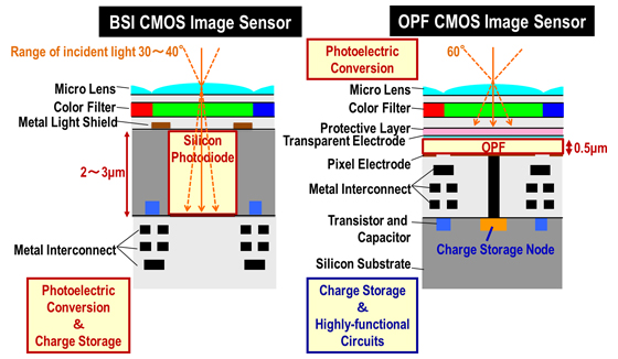
The conventional image sensor consists of a silicon photodiode for capturing light, metal interconnects and an on-chip micro-lens. And, both a photoelectric-conversion function and a signal charge-storage function are executed by a silicon photodiode. On the other hand, in an OPF CMOS image sensor, a photoelectric-conversion function is executed by an OPF, instead of a silicon photodiode, and a signal charge-storage function is executed by circuits beneath the OPF. Both functions are almost independent, so an OPF CMOS image sensor can achieve the following features.
Expansion of the incident light range to 60 degrees and reproduction of faithful color.
An OPF with high optical absorption coefficient [4], instead of a silicon photodiode, is adopted, the thickness of an OPF has been reduced to just 0.5 microns, four to six times thinner than silicon photodiodes. Since the conventional silicon photodiode needs at least 2 - 3 microns in depth, the range of incident angles was limited to around 30 - 40 degrees. An OPF, achieved with the OPF CMOS image sensor technology, has enabled the expansion of this range to 60 degrees, efficiently utilizing light entering at an angle for faithful color reproduction with no color mixing. It also gives greater flexibility in lens designs, facilitating the reduction of overall camera size.
Boost of sensor sensitivity by 1.2 times compared to conventional silicon image sensors to deliver clear images, particularly in dark conditions.
The transistors and metal interconnects in each pixel, fabricated using Panasonic's semiconductor device technology, are coated with an OPF. The area of the light receiving section becomes limited in conventional image sensors because of the existence of metal interconnects and the need to form a light shield film to prevent light incidence into areas other than the photodiode in each pixel. However, an OPF CMOS image sensor technology coats the sensor with an OPF, which can harvest all the light received on the sensor. This unique structure and high quantum efficiency of OPF boosts sensor sensitivity by 1.2 times compared to conventional silicon image sensors to deliver clear images, particularly in dark conditions.

Cross-sectional image of conventional Back Side Illumination (BSI) CMOS image sensor and OPF CMOS image sensor
Design of OPF and circuits completely independent and realization of high-performance (high-saturation)
In the architecture of an OPF CMOS image sensor, the OPF, that converts light into electric signals, and the circuits, that store electric signal charges and readout electric signals, are designed completely independently. Therefore, by selecting an OPF, photoelectric-conversion characteristics, wavelength, sensitivity, etc., can be set with flexibility.
Moreover, in conventional image sensors, it is necessary to place both a silicon photodiode and circuits (transistors and capacitors) on silicon substrate in each pixel, so an area of circuits is limited. On the other hand, in an OPF CMOS image sensor, it is not necessary to place a silicon photodiode, so high-performance circuits, such as high-speed or wide dynamic range, can be formed on a silicon substrate.
In particular, in an OPF CMOS image sensor, by providing a large capacitor for storing signal charge, a saturation value[5] of electric signal can be significantly increased from conventional image sensors*3
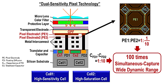
2.Dual-Sensitivity Pixel Technology that is provided with two sensitivity detection cells (one for brightness; one for darkness) in each pixel, taking advantage of a high-saturation performance and flexibility of a sensitivity setting of OPF CMOS image sensor, in order to achieve simultaneous-capture wide dynamic range.
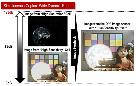
Two pixel electrodes with different sensitivities, two signal charge capacitors with different capacities and two types of noise cancellers in each pixel are provided, using OPF CMOS image sensor's particular pixel structure, in which an OPF, for photoelectric-conversion, and capacitor, for signal charge storage, are designed completely independently, and high-saturation value can be achieved. And, both bright scenes and dark scenes are imaged simultaneously using the different architecture's cells. So, 123dB simultaneous-capture wide dynamic range (that is 100x wider than that of common silicon image sensors*3) can be achieved.
Cell 1: high-sensitivity cell
high sensitivity pixel electrode + small storage capacitor
+ capacitive-coupling noise canceller
Cell 2: high-saturation cell
low sensitivity pixel electrode + large storage capacitor
+ conventional noise canceller
Using this technology, particularly in high-contrast situations, high-precision, high-speed imaging and motion detection can be realized.

Pixel Structure for achieving a wide dynamic range and its effect
In addition, the high-saturation cell of "Dual-Sensitivity Pixel Technology" always stores signal charge, in a state of low sensitivity, except during readout time. Therefore, neither LED Flicker[6] nor Fluorescent Flicker[7], that cause incomplete image capture problems in in-vehicle cameras, business broadcasting cameras, and so on, occurs.
3.Capacitive-Coupled Noise Canceller Technology that can cancel pixel reset noise, in order to improve S/N characteristics of imaging dark objects.
An OPF CMOS image sensor has a structure, in that an OPF and a charge storage part are connected with metal wire, so accumulating charges cannot be readout completely. Therefore, there is a problem with pixel reset noise, resting on the charge storage node, misleading readout with noise offset. To solve this problem, we have developed our own semiconductor device technology and a new and original " Capacitive-Coupled Noise Canceller ", and achieved cancellation of the reset noise itself. In this canceller, reset noise of each pixel can be suppressed by providing a negative feedback loop for each column. Furthermore, by using a capacitive-coupling structure, it is possible to improve the robustness of the negative feedback control and suppress reset noise significantly, up to 1.6 electrons.
Panasonic Corporation will apply this technology to surveillance camera, in-vehicle cameras, broadcasting cameras, industrial inspection cameras, digital still cameras and other imaging devices, and contribute to realize high-speed, high-precision imaging and sensing functions.
Technical Terms:
[1] Dynamic Range
Range of brightness that can be imaged.
(Ratio between the largest and the smallest values of brightness)
[2] Simultaneous-capture Dynamic Range
Range of brightness that can be imaged at a time.
[3] S/N
Signal to Noise Ratio, which represents the ratio of signal power to noise power.
[4] Optical absorption coefficient
A constant value that indicates how much light is absorbed into a material, when incident light enter to the material.
[5] Saturation Value
The maximum electrical signal quantity that can be handled.
If the signal exceeds this value, the image becomes overexposed.
[6] LED Flicker
Imaging phenomenon resulting in incomplete image capture, caused by a LED's (traffic, headlights, signs, etc.) frequency and a camera's imaging speed.
[7] Fluorescent Flicker
Imaging phenomenon resulting in incomplete image capture, caused by a Fluorescent lamp's (road lights, signs, etc.) frequency and a camera's imaging speed.

Captured image using by the new wide dynamic range technology
Panasonic Corporation is a worldwide leader in the development of diverse electronics technologies and solutions for customers in the consumer electronics, housing, automotive, enterprise solutions and device industries. Since its founding in 1918, the company has expanded globally and now operates 468 subsidiaries and 94 associated companies worldwide, recording consolidated net sales of 7.715 trillion yen for the year ended March 31, 2015. Committed to pursuing new value through innovation across divisional lines, the company uses its technologies to create a better life and a better world for its customers. To learn more about Panasonic: http://www.panasonic.com/global
The content in this website is accurate at the time of publication but may be subject to change without notice.
Please note therefore that these documents may not always contain the most up-to-date information.
Please note that German, Spanish and Chinese versions are machine translations, so the quality and accuracy may vary.