Feb 24, 2026
- Products & Solutions
- Press Releases
Jun 22, 2021
Products & Solutions / Press Releases
- This material improves the assembly-level reliability for state-of-the-art semiconductor packages
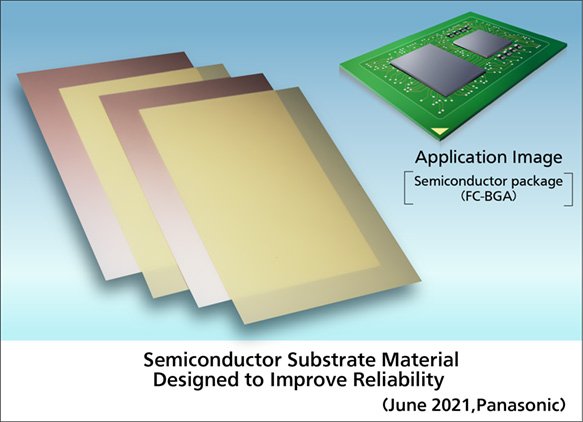
Osaka, Japan – Panasonic Corporation announced today that its Industrial Solutions Company has commercialized a semiconductor package substrate material (Product No. R-1515V) enabling both low package warpage and high assembly-level reliability. The newly developed material has very low thermal expansion properties to reduce warping of the substrate during the packaging process and optimized mechanical properties designed to lower the residual stress on solder joints created during reflow assembly. Mass production of the material will start in July 2021.
Semiconductors, the cornerstone of modern electronics, are critical to the advancement of IoT, AI, V2X, 5G and other leading-edge technologies. These devices have continued to improve and evolve in both die performance and packaging designs over time. The current generation of advanced package designs exhibit a relatively large footprint, a plethora of I/Os and high-density interconnecting structures like those found in 2.5D packages[1]. Along with the operating performance improvements, most industrial and commercial applications demand high assembly-level reliability from the assembled packages.
Panasonic has successfully developed many types of products for motherboard material and semiconductor packaging and assembly, including semiconductor package substrates; semiconductor encapsulation materials; and assembly-level reinforcement materials. By leveraging deep expertise in material technologies, the company has formulated a new semiconductor substrate material offering both low warpage and high assembly-level reliability. Improving chip packaging reliability requires reducing the substrate warpage during packaging, that is, mounting chips on the IC substrate followed by an encapsulation process. In addition, the stress imparted to the solder balls during the reflow assembly process -- during which the semiconductor package is assembled onto a motherboard -- needs to be lowered to ensure long-term operational reliability.
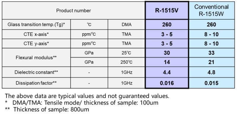
The coefficient of thermal expansion (CTE[2]) of this new substrate material is much closer to that of silicon IC chips, reducing warpage caused by the thermal excursions experienced during packaging processes. In addition, the new substrate material features excellent thickness tolerances, ensuring stable junctions between the substrate and the IC chips, further improving the reliability of packaged chip. The modified flexibility and buffering properties of the new material alleviate the stress on solder balls, improving the assembly-level reliability.
FC-BGA[3] packages, such as CPU[4], GPU[5], FPGA[6], and ASIC[7]
The product will be presented at the 2021 IEEE 71st Electronic Components and Technology Conference (from June 1 to July 4, 2021).
By using the resin design expertise honed over decades of electronic circuit board materials development, Panasonic has developed a material with a low thermal expansion coefficient of 4 ppm (measured by the company), close to the thermal expansion coefficient of silicon IC chips (semiconductors). This reduces warping caused by the difference in thermal expansion coefficient between the substrate and the IC chips and improves the reliability of mounting the IC chips on the substrate.
Based on simulation of modeling results, Panasonic developed a material combining flexibility and buffering properties by using internally developed resin design technology, while retaining low thermal expansion properties. This material absorbs and disperses the residual stress on the solder balls between the semiconductor package and the motherboard, which improves the reliability of SMT (Surface Mount Technology) assembly without affecting the quality of IC packaging.
With its precision resin flow control technology, which was established over decades of circuit board materials development, Panasonic has succeeded in ensuring laminated moldability while controlling resin flows, resulting in minimal thickness variations. This makes junctions between the substrate (core material) and the IC chips stable, further improving the reliability of IC chip packaging.
Electronic Materials Business Division, Industrial Solutions Company
https://industrial.panasonic.com/cuif/ww/contact-us?field_contact_group=2343&field_contact_lineup=3249&ad=press20210622ww
Panasonic Corporation is a global leader developing innovative technologies and solutions for wide-ranging applications in the consumer electronics, housing, automotive, and B2B sectors. The company, which celebrated its 100th anniversary in 2018, operates 522 subsidiaries and 69 associated companies worldwide and reported consolidated net sales of 6,698.8 billion yen for the year ended March 31, 2021. Committed to pursuing new value through collaborative innovation, the company uses its technologies to create a better life and a better world for customers. Learn more about Panasonic: https://www.panasonic.com/global.
The content in this website is accurate at the time of publication but may be subject to change without notice.
Please note therefore that these documents may not always contain the most up-to-date information.
Please note that German, Spanish and Chinese versions are machine translations, so the quality and accuracy may vary.