Feb 24, 2026
- Products & Solutions
- Press Releases
Jun 19, 2018
Products & Solutions / Press Releases
This new image sensor is capable of detecting objects 250 m ahead at night with poor visibility and achieves high resolution by adopting APD with 250,000 pixels
Osaka, Japan - Panasonic Corporation announced today that it has developed a time-of-flight (TOF) image sensor [2] that uses avalanche photodiode (APD) [1] pixels and is capable of capturing range imaging of objects up to 250 m even at night with poor visibility. The sensor can be applied in a variety of fields including automotive range imaging and wide-area surveillance in the dark.
The newly developed TOF image sensor directly measures the time-of-flight of light between an object and the sensor at all the pixels and collectively obtains 3D range images for short to long distances. The use of APDs, which amplify input signals, as the photodetector and the incorporation of an in-pixel circuit that integrates weak input signals, and it enables the 3D range imaging of a place 250 m ahead. In addition, the new sensor has achieved the integration of the world's best 250,000 pixels*1 through the lamination of the electron multiplier and the electron storage as well as the area reduction of APD pixels. This has enabled long-range and high-resolution 3D range imaging, which was difficult previously.
(As of Jun. 8, 2018, according to Panasonic data)
This development brings the following advantages.
(As of Jun. 8, 2018, according to Panasonic data)
Conventional camera technologies such as stereo cameras have an issue of degraded recognition accuracy at night. On the other hand, LiDAR that employs infrared light can be used at night; however, its low resolution makes it hard to identify small objects, which can cause missed detection.
Industrial/monitoring/automotive sensing cameras
This development result will be announced in the 2018 Symposia on VLSI Technology and Circuits, which will be held in Honolulu on June 20, 2018.
Conventional image sensors convert a single photon that has entered their pixels to only a single electron and therefore have an issue of being susceptible to noise when the signal light is as weak as approximately a single-photon level. The newly developed sensor forms very fine pixels of 11.2 μm pitch by using the APD pixel technology that laminates the photoelectric conversion region, multiplication region, and signal storage as constituents, thereby achieving a high resolution of 250,000 pixels and high sensitivity signals amplified by 10,000 times.
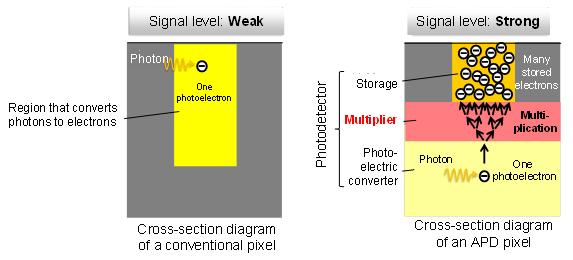
Fig.1 Comparison diagrams of the photodetector structure of a conventional image sensor and the APD image sensor
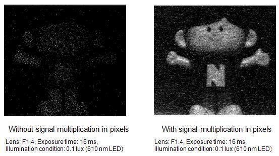
Fig. 2 Comparison diagrams of imaging with and without signal multiplication in pixels
Common TOF ranging calculates distances by measuring the time-of-flight of light emitted from a light source to hit an object, reflect, and return. Panasonic has developed a unique short-pulse TOF method that drives a high-speed 10-nanosecond shutter built in the sensor in sync with 10-nanosecond minimum short-pulse light. This newly developed technology enables the collective acquisition of a 3D range image by compositing multiple ranges from short to long.
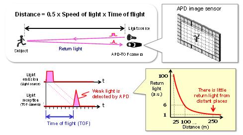
Fig.3 Explanatory diagram of the short-pulse TOF method
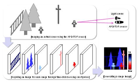
Fig. 4 Explanatory diagram of image acquisition by the APD-TOF sensor for each range using short pulses
Panasonic has developed APD pixel technology that enables fine pixels while possessing a multiplication function by providing a multiplication region that multiplies one photon to 10,000 electrons and laminating this multiplication region to accommodate it in the same plane area with the photoelectric conversion and signal storage regions. This technology enables sharp and high-resolution imaging in dark or distant places.
Panasonic has developed long-range measurement imaging technology that collectively obtains distance ranges from short to long as range images. The light reflected from a place 250 m away means that in terms of probability a signal of one photon barely arrives. The company has newly developed a weak light integration technology that reliably captures a weak signal of a single photon through the use of unique integration circuits built in all the APD pixels, which count the number of arrivals of photons. The long-range measurement imaging technology that combines the new short-pulse TOF method and weak light integration technology has achieved range images with both long-range measurement and high resolution at night, which was difficult for conventional stereo cameras and LiDAR. The new technology enables the acquisition of range images in which the position and shape of people and small objects, which are invisible to human eyes, can be discerned even at night from a long distance.
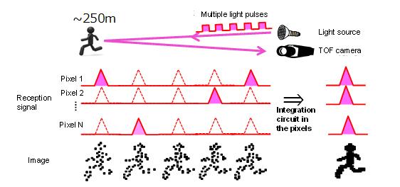
Fig. 5 Explanatory diagram of densification of weak light using the weak light integration technology
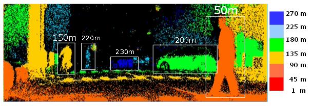
Fig. 6 3D range image obtained at night by the TOF image sensor
Panasonic Corporation is a worldwide leader in the development of diverse electronics technologies and solutions for customers in the consumer electronics, housing, automotive, and B2B businesses. Celebrating its 100th anniversary in 2018, the company has expanded globally and now operates 591 subsidiaries and 88 associated companies worldwide, recording consolidated net sales of 7.982 trillion yen for the year ended March 31, 2018. Committed to pursuing new value through innovation across divisional lines, the company uses its technologies to create a better life and a better world for its customers. To learn more about Panasonic:
https://www.panasonic.com/global.
Panasonic Corporation
Tel: +81-(0)3-3574-5664 Fax: +81-(0)3-3574-5699
The content in this website is accurate at the time of publication but may be subject to change without notice.
Please note therefore that these documents may not always contain the most up-to-date information.
Please note that German, Spanish and Chinese versions are machine translations, so the quality and accuracy may vary.