Nov 25, 2025
- Company
- Press Releases
- EV Solutions
- North America
- Automotive & Mobility
Feb 07, 2017
Company / Topics
Panasonic Factory Solutions Co., Ltd.
Tokyo Seimitsu Co., Ltd.
Panasonic Factory Solutions Co., Ltd. (Osaka, Japan, President: Hiroyuki Aota/hereafter "Panasonic Factory Solutions") and Tokyo Seimitsu Co., Ltd. (Tokyo, Japan, President and CEO: Hitoshi Yoshida/hereafter "Tokyo Seimitsu") have entered into a business tie-up to promote a "laser grooving and plasma dicing method" to enable the damage-free dicing of chips with metal layers, such as those used for sensors and memory, from wafers.
In the production of sensors and memory chips, pixel-size shrinkage and wafer thinning have led to issues with falling yields and the cracking of the chips. The "laser grooving and plasma dicing method" realizes higher yields by avoiding contamination in sensor production and achieves damage-free and higher-quality wafer thinning in memory chip production, with the superiority of the plasma dicing method.
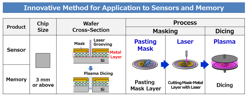
As shown in the figure below, in the case of a semiconductor chip with a metal layer, a "mask" is pasted for blocking purpose, and grooves of several tens of microns (μm) in width are formed. Plasma is then irradiated exclusively into the grooves needed for dicing the chips. A "laser grooving equipment" is designed to form these grooves using the laser-based precision processing technique.
Panasonic Factory Solutions and Tokyo Seimitsu will strive to create total solutions in dicing process for the future through strong partnership.
Panasonic Factory Solutions Co., Ltd.
Public Relations Section, Corporate Planning Group
TEL:+81-50-3487-3587
Tokyo Seimitsu Co., Ltd.
Public Relations Dept., Administration Company
TEL:+81-42-642-1701
The content in this website is accurate at the time of publication but may be subject to change without notice.
Please note therefore that these documents may not always contain the most up-to-date information.
Please note that German, Spanish and Chinese versions are machine translations, so the quality and accuracy may vary.