


Jul 01, 2026
- Company
- Press Releases
Oct 15, 2019
Company / Press Releases
Co-development of new high-value-added system to reduce engineering costs, stabilize product quality, and improve factory productivity
Osaka – October 15, 2019 – IBM Japan, Ltd. and Panasonic Corporation's subsidiary, Panasonic Smart Factory Solutions Co., Ltd. (hereafter "Panasonic"), announced today that the companies have agreed to collaborate to develop and market a new high-value-added system to optimize the overall equipment effectiveness (OEE) of customers' semiconductor manufacturing processes and to realize high-quality manufacturing.
As part of its circuit formation process business, Panasonic currently develops and markets edge devices and manufacturing methods that contribute to improving semiconductor manufacturing of advanced packaging. These new devices and methods include dry etching equipment, plasma dicers to produce high-quality wafers, plasma cleaners that increase metal and resin adhesion and high-accuracy bonding devices. This expertise will be combined with techniques and technology that IBM Japan has developed for semiconductor manufacturing to help Panasonic create smart factory technology. These include a data analysis systems including advanced process control (APC) and fault detection and classification (FDC), as well as an upper-layer manufacturing execution system (MES) — thus improving quality and automating production management in semiconductor manufacturing processes.
In recent years, IoT and 5G devices are becoming faster, smaller, and more multi-functional. This has given rise to manufacturing that is based on advanced packaging technology, in which a middle-end process (that combines the wafer process from the front-end process and the packaging technology from the back-end process) has been added between the front-end and back-end processes in semiconductor manufacturing.
Through the collaboration announced today, IBM Japan and Panasonic will jointly develop a data analysis system that will be incorporated into Panasonic's edge devices. The aim of this high-value-added system is to significantly reduce the number of engineering processes required, to stabilize product quality, and to improve the operating rates of manufacturing facilities. Specifically, the companies intend to develop an automatic recipe generation system for plasma dicers, which is a new advanced packaging production method that is drawing increased attention in the semiconductor manufacturing field, and a process control system that incorporates an FDC system in plasma cleaners — equipment that has demonstrated good results in the back-end process. Going forward, the new system and IBM Japan's MES will be connected to optimize OEE factory-wide and to realize high-quality manufacturing.
The two companies intend to develop the new system for the back-end process first, then explore an expansion of the scope to the front-end process in the future.
The computing algorithm jointly developed by the two companies enables customers to enter their desired dicing shape (etching shape), which varies from product to product, and automatically generate equipment parameters consisting of several hundred combinations. This feature is expected to significantly reduce product launch times and engineering costs. It can also be applied to the APC system, which automatically adjusts equipment parameters according to varying processing quality from front- and back-end processes; which will keep processed shapes stable, resulting in a high-quality dicing process.
FDC continuously accumulates operational data from operating manufacturing equipment, detects failures through its own data analysis method, and enables the condition of equipment to be interpreted automatically. This feature generates equipment maintenance target areas and frequency needs, forecasts and prevents failures, optimizes maintenance scheduling, reduces equipment downtime, and improves operating rates.
IBM has been a leader in the IT industry for more than 100 years and a leader in the semiconductor field in R&D of advanced miniaturization processing technology — delivering solid business results at 300 mm-semiconductor manufacturing plants across the world. Furthermore, as a solutions provider of production operation systems which enable non-stop full automation at factories, IBM has been contributing to the semiconductor manufacturing field for years. As semiconductors play a vital role in emerging technologies such as IoT and edge-computing, there are growing needs for greater sophistication and miniaturization of semiconductors. Working beyond conventional boundaries, IBM aims to promote the realization of smart factories through co-creation with Panasonic, thus providing new value to society.
Under its "Gemba Process Innovation" vision, Panasonic is expanding its B2B solutions business. The gemba, or physical site for frontline operations, refers to all places where products are made, moved or sold — the places where value is generated and problems must be confronted. By applying the company‘s 100-years of experience and expertise gained in the manufacturing industry with its sensing technologies and edge devices, Panasonic aims to co-create with its customers and partners to solve problems at the gemba. Panasonic is advancing the Gemba Process Innovation vision, aiming to become a total solutions integrator with offerings to the three main areas of manufacturing, logistics, and retail.
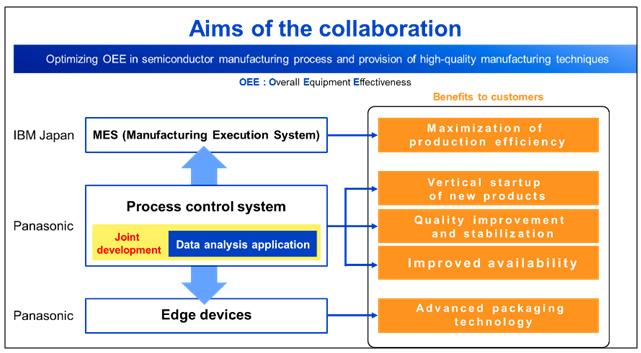 Aims of the collaboration
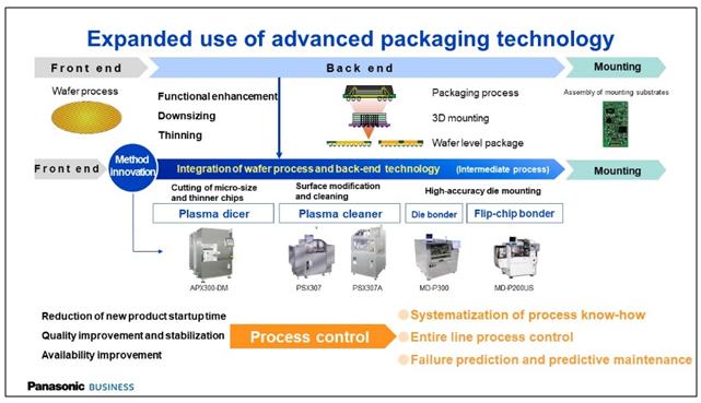 Expanded use of advanced packaging technology
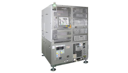 Panasonic APX300 Plasma Dicer (DM option)
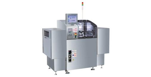 Panasonic PSX307 Plasma Cleaner
For more information on IBM Japan, visit https://www.ibm.com/ibm/jp/en/
Panasonic Corporation is a worldwide leader in the development of diverse electronics technologies and solutions for customers in the consumer electronics, housing, automotive, and B2B businesses. The company, which celebrated its 100th anniversary in 2018, has expanded globally and now operates 582 subsidiaries and 87 associated companies worldwide, recording consolidated net sales of 8.003 trillion yen for the year ended March 31, 2019. Committed to pursuing new value through innovation across divisional lines, the company uses its technologies to create a better life and a better world for its customers. To learn more about Panasonic: https://www.panasonic.com/global.
The content in this website is accurate at the time of publication but may be subject to change without notice.
Please note therefore that these documents may not always contain the most up-to-date information.
Please note that German, Spanish and Chinese versions are machine translations, so the quality and accuracy may vary.


