Feb 13, 2007
Press Release
FOR IMMEDIATE RELEASE
| Editorial Contact: | |
| Japan: Yoshinobu Sato Renesas Technology Corp. +81-3-6250-5554 sato.yoshinobu@renesas.com |
US: Akiko Ishiyama Renesas Technology America, Inc. +1(408) 382-7407 akiko.ishiyama@renesas.com |
| Contacts for Matsushita Electric Industrial | |
| Akira Kadota (Japan) International PR (Tel: +81-3-3578-1237) |
Chris De Maria (U.S.) (Tel: +1-201-348-7182) |
| Panasonic News Bureau (Japan) (Tel: +81-3-3542-6205) |
|
Renesas Technology and Matsushita Develop Technique for Stabilizing the Operation of On-Chip SRAM Manufactured with 45nm Process Generation Bulk CMOS
 (26KB)
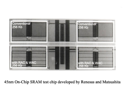
 TOKYO and SAN JOSE, Calif. ---February 13, 2007--- Renesas Technology Corp. and Matsushita Electric Industrial Co., Ltd. (NYSE:MC) today announced the development of a technique that achieves stable operation with 45nm (nanometer) process generation bulk CMOS*1 for SRAM (Static Random Access Memory) that can be embedded in SoC (system-on-a-chip) devices and microprocessors (MPUs). Tests of experimental chip with 512-Kbit SRAMs employing this technique have confirmed stable operation over a wide temperature range (-40°C to 125°C) and a larger operating voltage range margin with respect to process variations. The experimental SRAM chip, produced using a 45nm CMOS process, incorporated two different memory cell designs, one with a cell area of both 0.327µm2 and another with a cell area of only 0.245µm2 --- the world's smallest level. The smaller memory cell was achieved with a reduced processing dimension margin.
Details of this technology advance will be presented in paper 18.3 of Session 18 at the 2007 International Solid State Circuits Conference (ISSCC 2007) now being held in San Francisco. The innovation is of considerable significance because SRAM is an essential on-chip function for SoCs and MPUs used in embedded control applications. Conflicting trends see those applications becoming more sophisticated, requiring more SRAM, even as semiconductor process shrinks are making it more difficult to produce the stable SRAM operation necessary for proper device functionality. The 45nm process generation SRAM enabled by the new fabrication technique will make it possible to implement high-performance chips at low cost because it uses bulk CMOS instead of Silicon-on-Insulator (SOI) material, the more expensive alternative.
Overcoming problems caused by inevitable variations in threshold voltage
As LSI fabrication processes become finer, the increasing miniaturization causes greater variations of transistor characteristics, especially threshold voltage (Vth)*2, which can disrupt SRAM operation. Vth variation takes two forms. Global Vth variation occurs on a chip-by-chip or wafer-by-wafer basis due to minute disparities in transistor shape, such as gate length and gate width. Thus, it shows deviations in the same direction among chips. Global Vth variation previously has been the main challenge SRAM designers have had to overcome.
By contrast, local Vth variation is caused by fluctuation of the state of impurities in semiconductors, and arises even in adjacent transistors of the same shape. Therefore, it occurs randomly and without directivity. With the progress in transistor miniaturization, the problem of local Vth variation first manifested itself in the 90nm process generation. It is a major challenge that must be surmounted for embedded SRAM implemented in the 45nm process generation.
The semiconductor industry has been actively pursuing development of techniques for achieving stable SRAM operation. However, the problem of Vth variation as it affects the 45nm process has required further technical developments. The solution for a 6-transistor type SRAM memory cell that Renesas Technology and Matsushita have developed has two elements. One is a read-assist circuit that performs automatic adjustment linked to Vth variations. The other is a write-assist circuit that uses hierarchically structured power supply wiring.
The new read-assist circuit employs the resistance of passive elements in a compensation function that has a layout resembling that of the memory cell. Since memory cell variations and resistance value fluctuations are linked, the effects of Vth variations are reduced. The compensation function adjusts voltage automatically with respect to temperature and process variations. As a result, memory cell stability has been secured in read operations under a wide range of operating conditions, even if the symmetry of memory cell electrical characteristics degrades through increases in temperature and process variations.
The new write-assist circuit adds finer power supply lines (divided into eight) to the memory cell's column-unit power supply lines in a way that the isolation needed for the write operation is performed only where necessary. Also, it implements hierarchically structured power supply wiring. This reduces power supply line capacitance in critical areas, allowing the power supply line potential to be dropped to a low potential at high speed. Measurements on the experimental chip confirm that even under worst-case conditions (-40°C, minimum operating voltage, and worst-case process conditions), the new write-assist circuit provides a major improvement in SRAM write speed compared to an SRAM design in which it isn't used.
About Renesas Technology Corp.
Renesas Technology Corp. is one of the world's leading semiconductor system solutions providers for mobile, automotive and PC/AV (Audio Visual) markets and the world's No.1 supplier of microcontrollers. It is also a leading provider of LCD Driver ICs, Smart Card microcontrollers, RF-ICs, High Power Amplifiers, Mixed Signal ICs, System-on-Chip (SoC), System-in-Package (SiP) and more. Established in 2003 as a joint venture between Hitachi, Ltd. (TSE:6501, NYSE:HIT) and Mitsubishi Electric Corporation (TSE:6503), Renesas Technology achieved consolidated revenue of 906 billion JPY in FY2005 (end of March 2006). Renesas Technology is based in Tokyo, Japan and has a global network of manufacturing, design and sales operations in around 20 countries with about 26,200 employees worldwide. For further information, please visit http://www.renesas.com
About Panasonic
Best known by its Panasonic brand name, Matsushita Electric Industrial Co., Ltd. is a worldwide leader in the development and manufacture of electronic products for a wide range of consumer, business, and industrial needs. Based in Osaka, Japan, the Company recorded consolidated net sales of US$76.02 billion for the year ended March 31, 2006. The company's shares are listed on the Tokyo, Osaka, Nagoya and New York (NYSE:MC) stock exchanges. For more information on the Company and the Panasonic brand, visit the Company's website at http://panasonic.net/.
The content in this website is accurate at the time of publication but may be subject to change without notice.
Please note therefore that these documents may not always contain the most up-to-date information.
Please note that German, French and Chinese versions are machine translations, so the quality and accuracy may vary.