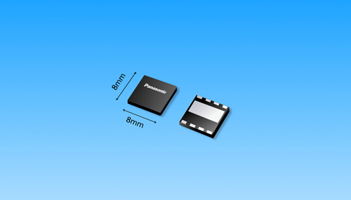
Osaka, Japan - Panasonic Corporation today announced that it will launch the industry's smallest enhancement-mode[1] gallium nitride (GaN)[2] power transistors (X-GaN™) package. The GaN is encapsulated into 8x8 dual-flat no-lead (DFN) surface-mount package. It is possible to mount the package on small area where it is difficult to mount conventionally and it is contribute to the reduction of the power consumption of industrial and consumer electronics equipment.
The breakdown voltage of the transistors is 600V in an enhancement mode, and the products have achieved a high-speed switching of 200V/ns and a low on-resistance[3] of 54 to 154 mΩ. The company will ship product samples, 10A type (PGA26E19BV) and 15A type(PGA26E08BV), in July 2015.
Power transistor is a semiconductor device to control power supply. GaN is one of remarkable semiconductor compounds and when it is applied to transistor, higher switching performance and higher break down voltage is expected than those of silicon (Si) and silicon carbide (4H-SiC).
Our conventional type of GaN power transistor is encapsulated into high heat diffusion surface-mount package TO220 (size:15 x 9.9 x 4.6mm), however the package is not enough to be small and it is limited the mounting area on the printed circuit board in the electronics equipment.
The parasitic inductance[4] reduce using surface mounting package and as a result the intrinsic GaN power transistor character, high switching performance, is brought out in smaller size 8 x 8 x 1.25mm under 600V high voltage. The power transistor is accelerated to introduce into electronics equipment and it contributes the reduction of the power consumption.
The products will be exhibited at Power Conversion Intelligent Motion 2015 (PCIM 2015) in Nurnberg, Germany from May 19 to 21, 2015.
[Features]
- Newly developed world's smallest GaN surface-mount package DFN 8x8 (8 x 8 mm x 1.25 mm, with a 43% footprint compared to our conventional TO-220 package products) optimized for GaN power transistors is employed.
- Adoption of a surface-mount package reduces parasitic inductance, achieving 200 V/ns high-speed switching performance.
- Panasonic's original gate injection transistors (GITs) [5] realized on a six-inch Si substrate allow creation of the enhancement mode.
* In the footprints of the 600-V enhancement-mode GaN power transistors as of May 18, 2015, according to a survey by Panasonic Corporation.
The GaN power transistors are applied to AC-DC power supply units (PFCs, insulated DC-DC converters), battery charging systems, PV power conditioners and EV inverters more easily.
The company holds 200 domestic patents and 180 overseas patents, including pending applications, such as US 8779438, the basic patent for its original GIT structure, and US 8299737, the basic patent for the driving system that takes advantage of normally-off operations.
This work is partially supported by the New Energy and Industrial Technology Development Organization (NEDO), Japan, under the Strategic Development of Energy Conservation Technology Project.
[Explanation of terms]
- [1] Enhancement mode
- An enhancement mode transistor is a single device transistor that is capable of realizing the normally-off characteristic, a characteristic of semiconductor devices that can prevent current flow between the source and the drain when no voltage is applied to the gate.
- [2] Gallium nitride (GaN)
- Gallium nitride is III-V compound semiconductor and has wide band gap (between valence band and conduction band). The larger band gap materials tend to be characterized with higher breakdown voltage.
- [3] On-resistance
- An on-resistance is a resistance between the source electrode and the drain electrode of a transistor when the transistor is turned on (conductive state).
- [4] Parasitic inductance
- Parasitic inductances are unintentional inductive components that exist in the packages of electronic parts. Although such inductances are not problematic with power supply units at a frequency of 50 or 60 Hz, they can be a substantial obstacle to high-speed operations with GaN power supply units operating at a frequency from several hundred kHz to several MHz.
- [5] GIT (Gate Injection Transistor)
- A GIT is a normally-off GaN transistor that was originally developed by Panasonic Semiconductor Solutions. New operating principles based on the increase in drain current at the time of hole injection are used to maintain the compatibility between low on-resistance and the enhancement mode.
GaN products webpage
http://www.semicon.panasonic.co.jp/en/products/powerics/ganpower/
About Panasonic
Panasonic Corporation is a worldwide leader in the development of diverse electronics technologies and solutions for customers in the consumer electronics, housing, automotive, enterprise solutions and device industries. Since its founding in 1918, the company has expanded globally and now operates 468 subsidiaries and 94 associated companies worldwide, recording consolidated net sales of 7.715 trillion yen for the year ended March 31, 2015. Committed to pursuing new value through innovation across divisional lines, the company uses its technologies to create a better life and a better world for its customers. To learn more about Panasonic: http://www.panasonic.com/global.
Media Contacts:
- Public Relations Department
- Panasonic Corporation
- Tel: +81-(0)3-3574-5664 Fax: +81-(0)3-3574-5699
- Panasonic News Bureau
- Tel: +81-(0)3-3542-6205 Fax: +81-(0)3-3542-9018