Osaka, Japan - Panasonic Corporation today announced that it has developed a low energy consumption circuit for neural network systems, by forming the world's first ferroelectric memristor[1], which can record continuous analog data as resistance, on a CMOS (Complementary Metal-Oxide Semiconductor) circuit. CMOS circuits are widely used as digital circuits. Devices equipped with this technology are able to handle digital signals as analog data in one circuit for the first time. Due to the direct processing of analog data, it is expected that the power consumption of neural network[2] circuits, which have the ability to carry out processing that replicates parts of human thought, such as the ability to make judgments based on broad trends, will decrease drastically to one tenth of the energy consumption of conventional circuits.
The resistance of a ferroelectric memristor can be changed continuously by an applied voltage. As the resistance is maintained without applying a voltage, it acts as a memory device. Therefore, as the device can store data as an intermediate value rather than a binary value (1/0), it is able to store more information than digital memory. Based on this large amount of information stored, through carrying out operations on the efficient analog data, it is possible to reduce the energy consumption as the amount of data to be processed increases. This development will contribute to the realization of a signal processing circuit which mimics the processing of neurons in the brain.
- Crystal growth technique for the forming of the ferroelectric memristor on a CMOS circuit through a seed layer[4].
- Hybrid circuit design to handle digital signals as analog data.
Panasonic holds 35 Japanese patents and 25 overseas patents, including pending applications, for this development.
A part of this technology will be presented at the 2013 Symposia on VLSI Technology and Circuits to be held at the Rihga Royal Hotel Kyoto, Japan on June 11-14.
More on the Technology
2. Hybrid circuit design to handle digital signals as analog data
A neural network circuit is a circuit that mimics the signal processing of a neuron in the brain. In this circuit, the information travels between multiple processing units as digital signals known as pulses. Analog processing using the pulses as a current is executed in the processing unit. Panasonic has developed a hybrid circuit design which can seamlessly carry out both digital and analog operations.
Notes
- [1] Ferroelectric memristor
- The resistance of a memristor is changed depending on the current passed through it. When the current is stopped, the memristor maintains the last resistance that it had. The memristor was originally theorized in 1971 by circuit theorists as the “fourth passive element" following resistors, capacitors and inductors. In June 2010, Panasonic had released that a similar function to a memristor can be realized by using a ferroelectric material. Panasonic calls this device as a "ferroelectric memristor".
- [2] Neural network
- At first, the weight values of the input signals are modified so that the output signals give the desired values. The weight values can be expressed as resistance. Since a ferroelectric memristor has large modulation range in its resistance, it is suitable for weighting in a neural network. After learning various data, the resistances of the memristors are fixed, and when unknown data is input, the data out of the learned data that is most similar to the input data is output. This makes immediate and flexible judgment possible.
- [3] Analog processing
- When digital signals are transferred through a ferroelectric memristor, if the resistance is low, a larger current flows. This corresponds to multiplication in the analog processing. When the current is charged in a capacitor, this corresponds to addition in the analog processing. Combining these elements, by charging the current from many ferroelectric memristors in a capacitor, a product-sum operation in the analog processing with low power consumption can be realized in a simple structure. As the amount of processing data increases, the reduction rate of the power consumption increases due to the efficient processing of analog data.
- [4] Seed layer
- The growth of a ferroelectric layer is strongly affected by the layer beneath. By forming an underlayer which has the same crystal structure and a close lattice constant as the ferroelectric film, a ferroelectric layer with a highly oriented crystal lattice was successfully formed. Since the underlayer acts as a seed for crystal growth, it is called a "seed layer."
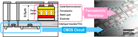
Schematic image of a test circuit,
which has ferroelectric memristors on the CMOS circuit substrate.
(Structural cross-section (left) and scanning electron microscope image (right))
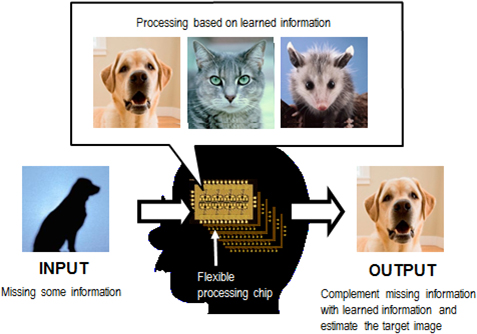
The image of the future information processing
with this developed technique.
About Panasonic
Panasonic Corporation is a worldwide leader in the development and engineering of electronic technologies and solutions for customers in residential, non-residential, mobility and personal applications. Since its founding in 1918, the company has expanded globally and now operates over 500 consolidated companies worldwide, recording consolidated net sales of 7.30 trillion yen for the year ended March 31, 2013. Committed to pursuing new value through innovation across divisional lines, the company strives to create a better life and a better world for its customers. For more information about Panasonic, please visit the company's website at http://panasonic.net/.